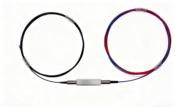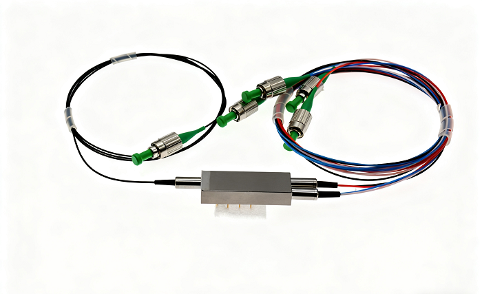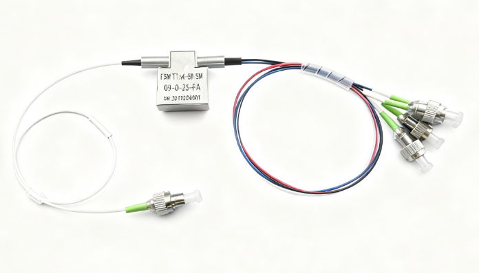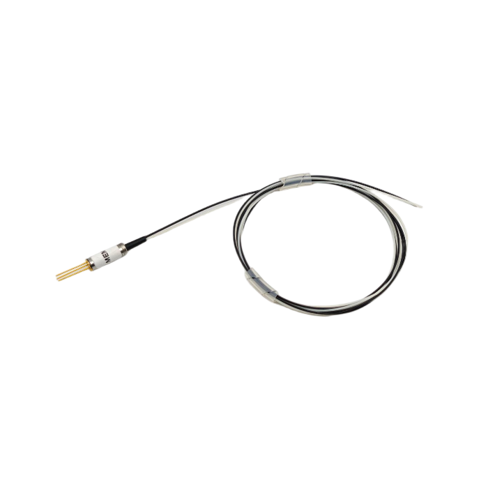
MEMS Polarization Maintaining 1×4 Optical Switch
This MEMS-based 1×4 polarization maintaining optical switch provides reliable and low-loss optical path switching for polarization-sensitive systems. It features high extinction ratio, low polarization-dependent loss, and fast switching time of ≤20ms, making it ideal for multi-channel optical monitoring, sensing networks, and test applications.
Operating at 1550nm with PM1550 fiber and FC/APC connectors, the switch supports TTL-level parallel control and offers long-term reliability with a lifespan of over 10 billion cycles. Its compact design and stable performance under varying temperatures make it suitable for demanding optical communication and measurement environments.
Description
I. Product Introduction
1. Application:
MFSW-1X6 optical switch type single mode optical switch module is a light path switching function of the device, which has the following purposes:
- Multiple optical monitoring in optical transmission system
- LAN multi-light source / detector automatic transfer, light sensing multi-point dynamic monitoring system
- Optical test system for optical fiber, optical devices, network and field engineering cable test
- Optical devices installed
2. Product Features:
- Low loss, high reliability
- Simple parallel or serial port interface control
- Modular design
3. Product Performance:
| Parameter | Specification |
| Working wavelength | 1550±20nm |
| Fiber type | PM1550(9/125) |
| Connector type | FC/APC(Slow axis alignment) |
| Fiber length | 500±50 mm |
| Insertion loss | ≤1.5dB |
| Return Loss | ≥50dB |
| Polarization dependent loss | ≤0.15 dB |
| Wavelength dependent loss | ≤0.3 dB |
| Temperature dependent loss | ≤0.3 dB |
| Min. Extinction Ratio | ≥15dB |
| Repeatability | ≤±0.05dB |
| Channel crosstalk | ≥50dB |
| Switching time | ≤15ms |
| Optical power | ≤500mW |
| Durability | ≥10 billion |
| Operating temperature | -5~+70℃ |
| Storage temperature | -40~+85℃ |
| Power supply | DC 5V ± 5% |
Ⅱ. The Appearance and Installation
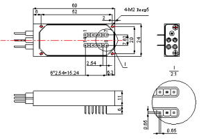
Figure 1 Dimensions
When installing the optical switch module, the optical fiber must not be bent excessively (refer to FIG. 2), so as not to affect the performance index of the optical switch module
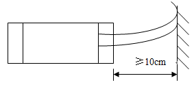
Figure 2 Optical installation diagram
Ⅲ. Pin Configure
1. Specification Digital Interface Electrical
| # | ELECTRICAL INTERFACE | SPECIFICATION |
| 1 | Supply Voltage | 5V ± 5% |
| 2 | Power Consumption | < 500 mW |
| 3 | Electrical control method | UART or Parallel mode (TTL level) |
2. Digital Interface Pin Assignment
| PIN # | NAME | DESCRIPTION |
| 1 | NC | No physical internal connection |
| 2 | VCC | Power Supply (5V) |
| 3 | STROBE | Falling Edge Active (input) |
| 4 | GND | Signal Ground |
| 5 | D0 | Data 0 (input) |
| 6 | D1 | Data 1 (input) |
| 7 | D2 | Data 2 (input) |
| 8 | D3 | Data 3 (input) |
| 9 | UART TX | UART Transmit (output) |
| 10 | UART RX | UART Receive (input) |
| 11 | GND | Case Ground |
| 12 | RDY | Ready (output), used for internal debugging |
| 13 | MODE | 0=TTL, 1=UART (input) |
| 14 | RESET | 0=Reset (input) |
Note:
- The digital interface is LVTTL level.
- Input control signal threshold level: Input logic high: 2V min. Input logic low:0.8V max
- All unused inputs of the device must be held at logic high or GND to ensure proper device operation.
Ⅳ. UART Interface
1. Specification Digital Interface Electrical
| Parameter | Value | Unit |
| Baud Rate | 115200 | Baud |
| Data Bits | 8 | Bits |
| Parity | None | |
| Stop bits | 1 | Bit |
| Flow control | None |
2. UART Protocol
Command/Response Format
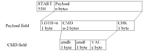
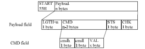
Command Format:<START><LGTH><cmdh><cmdl><VAL><CHK>
- <START> Start byte, for synchronization 0x55
- <LGTH> Num of characters in command, except <START> byte, including <LGTH>
- <cmdh> Command or data, high byte
- <cmdl> Command or data, low byte
- <VAL> Command parameter (in addition to show that with the parameters of the ASCII, other all use Hex)
- <CHK> One byte Checksum
Response Format: <START><LGTH><cmdh><cmdl><VAL><STS><CHK>
- <START> Start byte, for synchronizing 0x55
- <LGTH> Number of characters in command response except START byte, including <LGTH>
- <cmdh> Response command or data, high byte
- <cmdl> Response command or data, low byte
- <VAL> Command parameter
- <STS> Command execution status code
- <CHK> One byte checksum
Notes:
1)The command execution status code <STS> can have the following values:
| Statuscode | Description |
| 0x00 | Command executed successfully |
| 0x01 | Frame format error |
| 0x02 | Checksum error |
| 0x03 | Command parameter error |
| 0x04 | Execution failed |
| 0x05 | Execution timeout |
| 0x06 | Module is not ready |
| 0x07 | Command error |
| 0x08 | Device without calibration data |
| … | Reserved |
2)The <START> byte is used for synchronization. The module requires a 0x55 byte at the beginning of a command.
3)Checksumcalculation:
Send Check Byte = (LGTH⊕cmdh⊕cmdl⊕VAL)+1.
Return Check Byte = (LGTH⊕cmdh⊕cmdl⊕VAL⊕STS) +1.
For the above “⊕” is XOR.
4)In UART mode, the unit must receive a 0x55h byte to start up To avoid data loss, the device uses 0x55h as the frame head, and this means that 0x55 cannot be used again in the frame. Each 0x55h byte that appears in the framemust be replaced with the two bytes 0x56h0x56h. If a 0x56h appears in the frame it must be replaced with the two bytes 0x56h 0x57h.
| Data byte | Replaced with |
| 55h | 56h 56h |
| 56h | 56h 57h |
When replacements are made,the checksum calculation usesthe original data byte values.
Example:
Original data frame: 0x55, 0x05, 0x00, 0x02, 0x55, CHK
Sent data frame: 0x55, 0x06, 0x00, 0x02, 0x56, 0x56, CHK
The two frames will have the same CHK value, based upon the bytes in the original data frame.Expect the head byte is 0x55, other byte should not appear 0x55 in one frame, including LGTH and CHK bytes.
Example:
Original bytes: 0x55 0x08 0x80 0x10 0x0 0x0 0xFF 0x33 0x55
Corrected bytes (these are sent to the UART): 0x55 0x08 0x80 0x10 0x0 0x0 0xFF 0x33 0x56 0x56
5)When there is a frame format error or command error, the return frame does not necessarily need to return command parameters.
Example: Return data frame in event of frame format error or command error: 0x55 0x05 0x00 0x00 STS CHK
3. Command List
| Code | Description | Note |
| 0x0001 | Query manufacturer ID | Send command parameters: 0 bytes Return command parameters: 4 bytes |
| 0x0002 | Query module manufacturer name | Manufacturer name (up to 16 bytes, padded with zeros) Send command parameters: 0 bytes Return command parameters: 16 bytes(ASCII) |
| 0x0003 | Query module serial number | Module serial number Send command parameters: 0 bytes Return command parameters: 8 bytes (ASCII) |
| 0x0004 | Query module firmware version | Module firmware version Module firmware version: 7 bytes, format: x.xxTxxwhere x.xxTxx is a 7 character ASCII string. Send command parameters: 0 bytes Return command parameters: 7 bytes (ASCII) |
| 0x0005 | Query module hardware version | Module hardware version Module hardware version: 7 bytes, format: x.xxTxx where x.xxTxx is a 7 character ASCII string. Send command parameters: 0 bytes Return command parameters: 7 bytes (ASCII) |
| 0x0006 | Query module production date | Module production date Production date: 10-byte format: xxxx-xx-xx (Year-Month-Day separated by “-“ characters) Send command parameters: 0 bytes Return command parameters: 10 bytes(ASCII) |
| 0x0007~0x0009 | Reserved | |
| 0x0010 | Set the optical switch channel | Switch channel Send command parameters: 1 byte (Switch channel) Return command parameters: 0 bytes Switch Channel Range: 0~7 and 0xFF 0 represents channel 1. 0xFF represents dark channel. |
| 0x0011 | Query the optical switch channel | Switch channel Send command parameters: 0 bytes Return command parameters: 1byte(Switch channel) Switch Channel Range: 0~7 and 0xFF 0 represents channel 1 0xFF represents dark channel. |
| 0x0012~0xffff | Reserved |
Notes:
- Value of optical switch channels: 0~7 and 0xFF,default is dark channel.
- Command examples:
Query manufacturer ID:
Send 0x55,0x04,0x00,0x01,CHK
Return 0x55,0x09,0x00,0x01,ID_hh,ID_hl,ID_lh,ID_ll,STS,CHK
Query module firmware version:
Send 0x55,0x04,0x00,0x04,CHK
Return 0x55,0x0c,0x00,0x04,FW_maj,0x2e,FW_hh,FW_hl,0x54,FW_lh,FW_ll,STS,CHK
Set the optical switch channel:
Send 0x55,0x05,0x00,0x10,channel,CHK
Return 0x55,0x05,0x00,0x10,STS,CHK
Query the optical switch channel:
Send 0x55,0x04,0x00,0x11,CHK
Return 0x55,0x06,0x00,0x11,channel,STS,CHK
Ⅴ. Parallel Mode
1. Control Truth Table
| Select CH | PIN# | Comment | |||
| D3 | D2 | D1 | D0 | ||
| Default | N/A | N/A | N/A | N/A | Default CH is off(*) |
| P1 | 0 | 0 | 0 | 0 | |
| P2 | 0 | 0 | 0 | 1 | |
| P3 | 0 | 0 | 1 | 0 | |
| P4 | 0 | 0 | 1 | 1 | |
| P5 | 0 | 1 | 0 | 0 | |
| P6 | 0 | 1 | 0 | 1 | |
| (*1)When power(VCC)is removed from the switch, it will go go the off(dark) position. | |||||
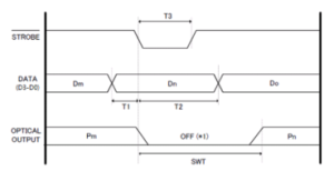
2. Control Timing Parameters
| Symbol | Parameter (TTL mode) | Min. | Typ. | Max. | Unit |
| T1 | Data setup time | 1 | ms | ||
| T2 | Data hold time | 10 | ms | ||
| T3 | Strobe pulse width | 1 | ms | ||
| SWT | Optical output switching | 50 | ms |
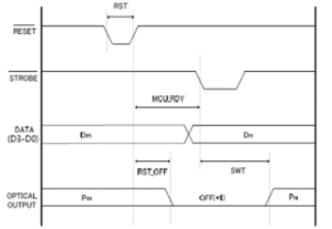
3. Reset Control Timing
| Symbol | Parameter | Min. | Typ. | Max. | Unit |
| RST | Reset pulse width | 100 | ms | ||
| MCU_RDY | MCU Ready | 20 | ms | ||
| RST_OFF | Reset Power OFF | 30 | ms |
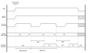
Power/STROBE Sequence
| Symbol | Parameter (TTL mode) | Min. | Typ. | Max. | Unit |
| PWR_UP_RDY | Power up Ready | 200 | ms | ||
| CMD_CYC | Command Cycle | 50 | ms |
Ⅵ. Precautions
Before using the optical switch module, in order to avoid any damage to the optical switch module, please read the following rules carefully:
- Before use, clean the optical fiber end of the connector with alcohol cotton. Please take a dust cap when not in use to prevent the dust or other dirt from polluting or damaging the fiber end face. Fiber end damage or contamination will affect the optical switch module performance.
- Do not pull, fold and twist the optical fiber, so as to avoid fiber damage.
- Detailed pin definition for control interfaces, to ensure that the connection is correct. After determining the connection is correct, then power-up operation.
- When the external circuit needs to be changed, please turn off the power, then disconnect the module control line, the control line is prohibited with hot-swappable.
- Do not look directly at the fiber end when the optical switch module has an optical signal input. Laser radiation is not visible, but will cause harm to the human eye!
- The device should be fireproof, shockproof, to avoid storage and work in an over-humid environment.
- The device is a precision optical device, shall not be disassembled, so as not to damage.