Enabling the Optical Revolution: Precision Lensed Fibers for Scalable Silicon Photonics Testing
The Drive Towards Optical Interconnects
The exponential growth of artificial intelligence, cloud computing, and high-performance computing is fundamentally reshaping data center infrastructure. With a single AI query consuming significantly more power than a traditional search, the industry faces an urgent need for more efficient data transfer technologies. Silicon Photonics (SiPh) and Co-Packaged Optics (CPO) have emerged as the leading solutions, promising substantial reductions in power consumption—up to 30% or more according to industry leaders—while delivering unprecedented bandwidth and lower latency.
However, the mass adoption of these advanced optical technologies is not solely dependent on chip design and packaging. It hinges on overcoming formidable testing and manufacturing challenges, particularly in achieving reliable, high-precision optical connections at an industrial scale. This is where specialized optical components, particularly advanced lensed fibers, become critical enablers for the industry’s future.
Key Testing Challenges in Silicon Photonics and CPO Manufacturing
The transition from electrical to optical interfaces introduces a new paradigm in semiconductor testing, characterized by extreme precision and complexity:
- Sub-Micrometer Alignment Precision: Testing photonic integrated circuits (PICs) at the wafer level requires optical fibers to be aligned with on-wafer couplers with sub-micrometer accuracy. This is orders of magnitude more precise than the tens-of-micrometer alignment typical in electrical probing. Any misalignment leads to inaccurate power measurements and signal loss.
- High-Speed Performance Validation: Devices must be validated at operational speeds, often with data rates of 112 Gbps or 224 Gbps PAM4. This demands robust optical connections that can facilitate loopback testing or interface with high-speed test equipment without introducing errors.
- Scalability for High-Volume Production: While current pluggable transceiver volumes are in the millions annually, CPO adoption is expected to drive optical engine production into the hundreds of millions. Manual or semi-custom testing methods cannot scale to meet this demand, necessitating fully automated, precision-aligned test cells.
Precision Lensed Fibers: The Critical Interface for Testing and Integration
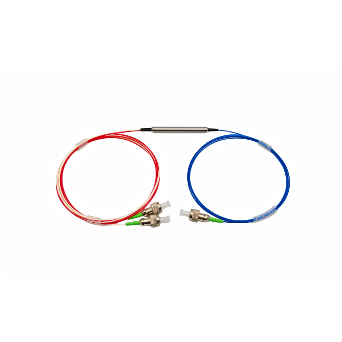
Addressing these challenges requires more than just standard optical fibers. It demands engineered interface solutions designed for specific optical performance. Feiyi Photonics’ portfolio of specialized lensed optical fibers provides this vital link, offering tailored solutions for the most demanding test and integration scenarios in SiPh and CPO.
The company’s expertise lies in the precision grinding and polishing of fiber endfaces into specialized geometries, followed by the application of custom optical thin films. This technical capability directly addresses the core pain points in optical testing:
| Lensed Fiber Type | Key Feature & Manufacturing Process | Primary Application in SiPh/CPO Testing & Integration |
|---|---|---|
| Angled Lensed Fiber | Endface polished at a specific angle; optical coatings applied to reduce back reflection. | Minimizing signal interference and insertion loss during loopback and high-speed testing. Critical for accurate Bit Error Rate (BER) measurements. |
| Custom Geometry Lensed Fiber | Endface processed into conical, multi-facet, or spherical shapes to control spot size and beam path. | Optimizing coupling efficiency between test equipment and on-chip couplers (grating couplers, edge couplers). Essential for achieving high-yield wafer-level probing. |
| Fully Customized Solutions | Tailored endface geometry combined with application-specific optical coatings. | Solving unique alignment challenges, interfacing with non-standard optical connectors, and enabling passive alignment in advanced packaging. |
Enabling Scalable, High-Volume Test Solutions
The true value of these precision components is realized when they are integrated into automated test ecosystems. As highlighted in industry analysis, the future lies in thousands of automated “optoelectronic” test cells within foundry and OSAT facilities. These cells must be operable by production staff, not just optical engineers.
Reliable, standardized lensed fiber interfaces are fundamental to this vision. They provide:
- Repeatable Connections: Ensuring every automated probe or connector delivers consistent optical performance, test after test.
- Robustness for Production Environments: Designed to withstand the rigors of high-volume manufacturing floors.
- Flexibility: Custom geometries allow test system designers to optimize for different PIC designs and packaging approaches, overcoming the industry’s current lack of connector standardization.
The Path Forward
The synergy between advanced test systems, like those being developed by industry leaders, and precision optical components is unlocking the future of computing. As CPO designs evolve to integrate dozens of optical engines around a single compute die, the demand for reliable, high-density optical interconnect solutions will only intensify.
Feiyi Photonics, through its deep expertise in optical fiber processing and coating technology, is positioned as a key partner in this optical revolution. By providing the critical lensed fiber interfaces that enable scalable testing and efficient integration, we are helping to turn the promise of silicon photonics and co-packaged optics—lower power, higher bandwidth, and scalable AI infrastructure—into a commercial reality.
https://www.feiyi-oeo.com/product-category/passive-device/lensed-optical-fibers